A Chinese tech firm in Wuhan, Hubei province, has achieved a breakthrough in mass-producing silicon carbide (SiC) wafers at record speeds by using lasers instead of diamond wires. This marks a major technical advancement for electric vehicle makers working on faster charging systems. [Photo by Wei Lai/Provided to chinadaily.com.cn]
A Chinese tech firm in Wuhan, Hubei province, has achieved a breakthrough in mass-producing silicon carbide (SiC) wafers at record speeds by using lasers instead of diamond wires. This marks a major technical advancement for electric vehicle makers working on faster charging systems.
SiC ingots, a third-generation semiconductor material, outperforms traditional silicon in high-voltage and high-temperature environments, making it a key component in next-generation electric vehicles that demand faster charging and longer range.
Traditionally, SiC ingots were cut using 100-micrometer diamond wires, a method akin to slicing a carrot. From a 1-cm-thick ingot, only 10 wafers (each 500 μm thick) could be produced, with each cut taking 24 hours and resulting in 50 percent material loss.
In response, Si LAL, the tech firm in Wuhan, has developed laser spalling technology. Instead of "cutting", it uses ultra-precise lasers to focus energy a billion times inside the ingot, altering the SiC structure and "peeling" wafers off layer by layer, similar to how sunlight causes skin to peel.
The challenge lies in ensuring uniform wafer thickness, requiring nanoscale precision in laser focus depth. Thus, Si LAL developed a hybrid laser system, achieving 100 percent domestic control over hardware and software and placing China at the global forefront of SiC wafer production.
The results showed that the company can produce 15 to 16 500-μm-thick wafers in every 1-cm-thick ingot. The time required for each wafer has been reduced to 15 minutes, and material loss has been reduced to 15 percent. The cost per wafer has been slashed by more than 20 percent, and the yield rate exceeds 99 percent.
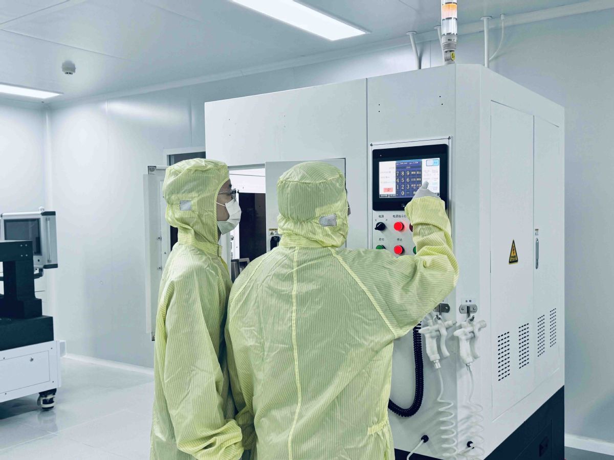
In May, the company's first SiC wafer cutting production line was put into operation in Optics Valley, a high-tech development zone in Wuhan, with an annual production capacity expected to exceed 30,000 wafers.
Si LAL plans to build four or five new production lines in Wuhan to create an expected annual output value exceeding 1 billion yuan ($139 million).
Editor: Zong Xia
